An Scr Has Pn Junctions
Chua and Kang later. A portmanteau of memory resistor is a non-linear two-terminal electrical component relating electric charge and magnetic flux linkageIt was described and named in 1971 by Leon Chua completing a theoretical quartet of fundamental electrical components which comprises also the resistor capacitor and inductor.

Definition Of Pn Junction Pcmag
The p-type and n-type regions are typically heavily doped because they are used for ohmic contacts.
. Field-testing semiconductor devices focuses on using an. Steady state I-V characteristics under forward bias reverse bias and illumination. The channel is used for the flow of majority charge carriers.
This is helpful for the users who are preparing for their exams interviews or professionals who would like to brush up their fundamentals on the Sensors topic. Duty classes S1 S10 and IP class. Thyristor SCR has the turn-off time in the order of microseconds about 5 μs.
Enter the email address you signed up with and well email you a reset link. Diffusion lengthQuantitative theory of PN junctions. It is a four-layer PNPN device having three PN junctions.
They work like a bistable switch and it operates from nonconducting to conducting. A Varactor diode is a reverse-biased p-n junction diode whose capacitance can be varied electrically. Signals and Amplifiers 4 CHAPTER 2 Semiconductors 124 CHAPTER 4 MOS Field-Effect Transistors MOSFETs 230 Bipolar Junction Transistors BJTs 350 Devices and Basic Circuits.
Power circuit operation continuous and discontinuous conduction. BJT has the turn-off time in the order of nanoseconds to microseconds. The triac is a.
It includes three terminals namely anode gate and cathode. It has three terminals Gate G CollectorC and Emitter E. When the gate pulse is removed from an SCR the SCR will stop conducting.
The thyristor or SCR is a power semiconductor device which is used in power electronic circuits. A power diode has a P-I-N structure as compared to the signal diode having a PN junction. To determine if PN junctions in the device are functioning properly.
A half-wave rectifier has an input voltage of 240 V rms. DC Drives SCR bridge 3-phase based drive. SCR usually has three terminals and four layers of alternating p.
A PIN diode is a diode with a wide undoped intrinsic semiconductor region between a p-type semiconductor and an n-type semiconductor region. This article lists 100 Sensors MCQs for engineering studentsAll the Sensors Questions Answers given below include a hint and wherever possible link to the relevant topic. Has three leads identified as gate main terminal 1 and main terminal 2.
For this type of diodes the N-type silicon semiconductor has an extra electron which is required by the p-type silicon. The one end of a symbol consists of the diode and the other end has two parallel lines that represent the conductive plates of the. It has the ability to control huge current and is generally used.
A memristor ˈ m ɛ m r ɪ s t ər. A thyristor is a four-layer solid-state semiconductor device that contains 3 PN junctions in series having 3 terminals called anode cathode and gate. The anode and cathode terminals are placed at the end layers and where the gate terminal is placed with the third layer.
The terminals name also implies being taken from both transistors. One PN junction between Collector and Base and the other between Base and Emitter. These four-layer form three PN junctions named J1 J2 and J3.
Like a diode a thyristor is a unidirectional device as well but unlike diode it can be used as an open circuit switch. SCR has four layers of extrinsic semiconductor materials. The designing of thyristors can be done with 3-PN junctions and 4 layers.
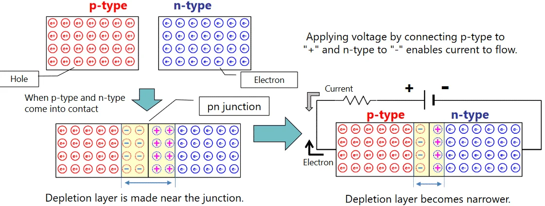
Therefore the electrons migrate from the n-type material to the p-type material across the junction through the process of diffusion. The outer layers are heavily dopped and the inner. IGBT has the turn-off time in the order of microseconds about 1 μs.
Here the I in P-I-N stands for intrinsic semiconductor layer to bear the high-level reverse voltage as compared to the signal diode the n-drift region layer shown in Figure 1. BJT transistor has two PN junctions between its collector and emitter. These diodes are also known as varicaps tuning diodes voltage variable capacitor diodes parametric diodes and variable capacitor diodes.
The wide intrinsic region is in contrast to an ordinary pn diodeThe wide intrinsic region makes the PIN diode an inferior rectifier one. FET has either an N-channel or a P-channel between the gate of the P-layer or the N-layer respectively. Therefore the increasing order of turn-off times is.
Gate terminal as it is the input part taken from MOSFET while the collector and emitter as they are the output taken from the BJT. The layers are either NPNP or PNPN. If the step-down transformer has a turns ratio of 81 what is the peak load voltage.
MOSFET has the lowest switching off time in the order of nanoseconds.
P N Junction Diodes Everything You Need To Know
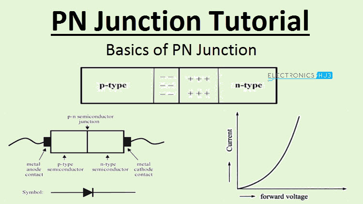
Pn Junction Tutorial Introduction To Pn Junction Diodes
P N Junction Showing Formation Of The Space Charge Region Scr Download Scientific Diagram

How Is Pn Junction Formed Basics And Examples
No comments for "An Scr Has Pn Junctions"
Post a Comment